Patterned Wafer Inspection System

5 Wafer Defect Inspection System Hitachi High Tech Global

Patterned Wafer Inspection

Semiconductor Wafer Defect Inspection Reliant Systems Inc

Optical Patterned Wafer Inspection Tool Market To Escalate News

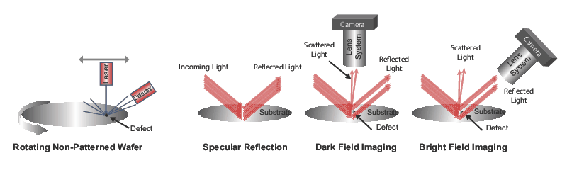
Inspecting Unpatterned Wafers

Kla Introduces Breakthrough Electron Beam Defect Inspection System

This kla tencor sfs 7600 surfscan patterned wafer inspection system is used and in good condition.
Patterned wafer inspection system.
Semiconductor Inspection

Kla Tencor Announces Defect Inspection Systems News

Wafer Inspection System 390x Series Kla Tencor Surface Defect
Wafer Inspection System Inspectra Series Optical Semiconductor Wafer Inspection System Product Information Tasmit Inc

Silicon Manufacturing How Wafers Are Inspected

Inspection System Zi 2000 Screen Semiconductor Solutions Co Ltd

Dark Field Wafer Defect Inspection System Is Series Hitachi High Tech Global

Optical Inspection System 8 Series Kla Tencor Scanning For Wafers Led

Optical Inspection Machine Puma 9980 Kla Tencor For Patterned Wafers Defect

Kla Tencor Sfs 7600 Surfscan Patterned Wafer Inspection System Price Specs

Wafer Inspection Standards
Kla Tencor Ait I Patterned Surface Defect Inspection System Classone Equipment

Wafer Surface Inspection System Ls Series Hitachi High Tech In America

Video 1 Kla Tencor 2139 Brightfield Patterned Wafer Inspection System Id 3735 Youtube
Fabexchange Auctions Kla Tencor 7700 Surfscan Patterned Wafer Inspection System

E Beam Inspection Makes Inroads

Optical Inspection Machine 29xx Series Kla Tencor For Patterned Wafers High Resolution Defect
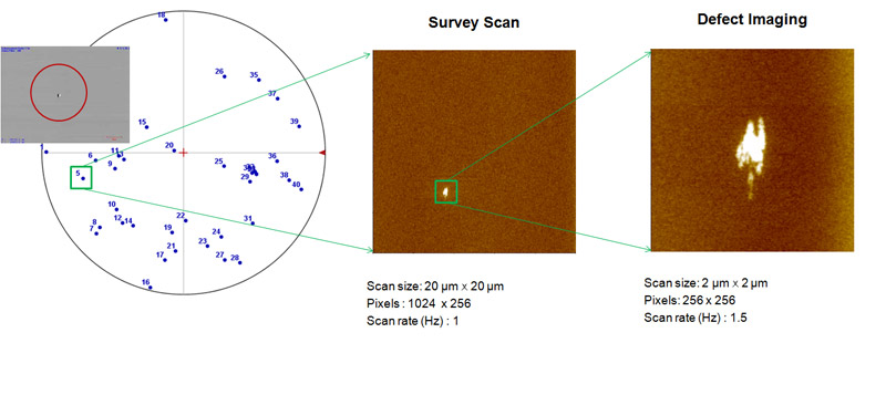
Automatic Defect Review Adr Of 300mm Bare Wafers With Automated Afm
Https Encrypted Tbn0 Gstatic Com Images Q Tbn 3aand9gcsvtra Yd3hz9k5q4foguz0eru Avnnz2dainias1s Usqp Cau

Principle Of The Patterned Wafer Defect Inspection Adapted From 8 Download Scientific Diagram

Core Business More Information Lasertec Corporation

Metrology Inspection Systems Spec Equipment

Kla Announces New Defect Inspection And Review Portfolio News

Spec Equipment Kla Tencor Model Ait Xp Darkfield Inspection System
Source : pinterest.com
