Pcb Design Process Steps Pdf

Pcb Circuit Board Fabrication Process Flow Process Flow Pcb Circuit Board Circuit

Top 10 Free Pcb Design Software Gadgetronicx Pcb Design Software Pcb Design Software Design

Download Complete Pcb Design Using Orcad Capture And Layout Pcb Design Circuit Board Design Printed Circuit Boards
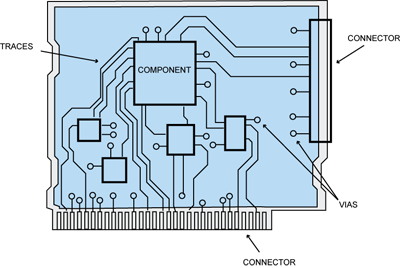
Printed Circuit Board Design Diagram And Assembly Steps Tutorial

Pcb Design And Layout Circuitsify

A Flow Chart To Understand Pcb Designing Process
The pcb design process a summary of a lot of information place components route traces fab.
Pcb design process steps pdf.

Getting Started With Pcb Design Altium Com
Learnemc Pcb Layout

Pcb Reverse Engineering Expert Pcb Copy Engineering Service

Pcb Layout Basics Component Placement Eagle Blog

The 3 Essentials Of Pcb Design Testing Tempo

Printed Circuit Board Timeline Circuit Board Printed Circuit Board Printed Circuit Boards

Nanino The Diy Friendly Arduino Arduino Arduino Pcb Arduino Projects

Complete Pcb Design Using Orcad Capture And Pcb Editor By Kraig Mitzner Pcb Design Printed Circuit Boards Circuit Board Design

12 To 220v Inverter Pcb Electronic Circuit Design Electronic Circuit Projects Pcb Design

Making A 4 Channel Rf Remote Pcb Design Included Gadgetronicx Pcb Design Remote Remote Control

Printed Circuit Board Prototype With Images Circuit Board Design Printed Circuit Board Printed Circuit

Step By Step Example For Practical Pcb Design Power Supply Design Tutorial Section 3 3 Power Electronics News

Pcb Assembly 101 Hax Printed Circuit Board Circuit Board Design Printed Circuit

10 Free Pcb Design Software Pcb Design Software Pcb Design Electronic Engineering

500w Amplifier Pdf Circuit Diagram Audio Amplifier Circuit
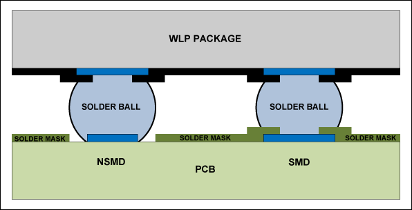
Pcb Design Considerations And Guidelines For 0 4mm And 0 5mm Wlps
Pcb Design Basics 101 Beginners Guide Get Started With Basics Of Pcb

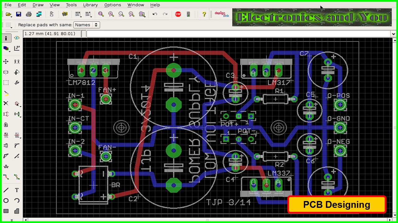
Pcb Designing How To Design A Pcb Step By Step In 2020 Electronics Projects Diy Technology Systems Design
Https Encrypted Tbn0 Gstatic Com Images Q Tbn 3aand9gcrfd37hr2roshpovm7oqhucwpy9bo Dhgf0mc9seqcfdogarnoe Usqp Cau

Pcb Assembly Process Step By Step Guideline Circuit Board Printed Circuit Boards Circuit Board Design

Englishexam Englishforyou Englishidioms Englishspeaking Englishforchildren Learningenglish Englishlangua Learn English Book Publication Electronic Books

Top 10 Free Pcb Design Software Gadgetronicx In 2020 Pcb Design Software Pcb Design Software Design

Pcb Design How To Create A Printed Circuit Board Pcb Design Electronics Circuit Pcb Design Software

Top 10 Free Pcb Design Software Pcb Design Software Software Design Pcb Design
Source : pinterest.com
